
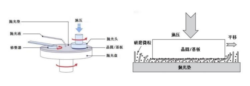
CMP, or Chemical Mechanical Polishing, is a process that uses chemical etching and mechanical force to planarize silicon wafers or other substrate materials during manufacturing. The equipment comprises three main modules: polishing, cleaning, and transfer. During the process, the polishing head presses the wafer surface to be polished against a rough polishing pad, achieving global planarization through coupling via the etching of the polishing slurry, particle friction, and friction from the polishing pad. Modern integrated circuit components generally employ multi-layered, three-dimensional wiring, thus requiring multiple cycles in the front-end processes of integrated circuit manufacturing. In this process, CMP technology is a key process for achieving wafer surface planarization in integrated circuit (chip) manufacturing and a crucial step in advancing process technology nodes in integrated circuit manufacturing.
CMP materials, based on their functions, are mainly categorized into polishing slurries, polishing pads, post-polishing cleaning solutions, and conditioning agents. Polishing pads primarily store and transport the polishing slurry, remove abrasive debris, and maintain a stable polishing environment. During chemical mechanical polishing (CMP), the polishing slurry creates an oxide film on the wafer surface, which is then removed by the abrasive particles in the slurry, achieving the polishing purpose. Cleaning solutions are mainly used to remove residual dust particles, organic matter, inorganic matter, metal ions, oxides, and other impurities from the wafer surface.
The polishing slurry is a water-soluble reagent composed of deionized water, abrasive particles, pH adjusters, oxidants, and dispersants. During polishing, the oxidants and other components in the slurry react chemically with the silicon wafer surface material, forming a chemical reaction film. This film is then removed by the abrasive particles in the slurry under pressure and friction, ultimately achieving polishing.
In fact, the applications of CMP polishing slurries in the integrated circuit field extend far beyond wafer polishing. CMP processes used in semiconductors include oxide CMP, polysilicon CMP, and metal CMP. Regarding polishing processes, different manufacturing processes require different polishing procedures. The 28nm process requires 12-13 CMP cycles, while the number of CMP cycles doubles to 25-30 cycles with the 10nm process.
1. Shallow Trench Isolation Planarization (STI CMP)
Shallow Trench Isolation (STI) technology uses oxide to separate individual gate circuits, preventing them from conducting to each other. The goal of STI CMP is to remove excess dielectric filling the shallow trenches and separate two adjacent active device regions by creating dielectric isolation between transistors. As technology advances to more advanced nodes, the performance requirements for STI CMP become more stringent due to the smaller distance between transistor regions.
The most important process performance in the first step of STI CMP is ensuring the uniformity of the oxide film and minimizing scratches. The second step is to remove the remaining oxide and expose the active nitrides, while simultaneously creating as few depressions as possible in the oxide within the trenches. Because the second step of CMP involves direct contact with the nitrides, any polishing scratches can be detrimental to device quality and ultimately affect wafer yield.
2. Interlayer Dielectric Planarization (ILD CMP) The dielectric layer is the electrically insulating layer between silicon devices and metal layers, and between metal layers themselves. Also known as the interlayer dielectric (ILD), SiO2 is the most common interlayer dielectric, used as an insulating film or isolation layer. Its flatness affects the subsequent manufacturing of metal layers. The main purpose of ILD CMP is to planarize the ILD oxide layer, primarily by grinding silicon dioxide (Oxide) to a certain thickness to achieve planarization.
3. In-Metal Dielectric Planarization (IMD CMP) With the increasing integration density of integrated circuits, more layers of metal interconnects are needed to connect the various components within a microprocessor. During the connection process, direct contact between metal lines must be avoided to prevent short circuits. Insulators must be used to isolate the metal layers. The dielectric material used to isolate the metal layers is called the "intermetallic dielectric layer." SiO2 is commonly used as the interlayer dielectric; therefore, the IMD CMP process is similar to the ILD CMP process.
4. Polysilicon Planarization (Poly CMP): The trenches from the STI process are deepened. Silicon oxide or silicon nitride is deposited using CVD, and then polysilicon is used as the depositing material. CMP removes excess polysilicon outside the deep trenches, and the silicon oxide or silicon nitride film grown on the silicon wafer and within the trenches serves as the polishing stop layer, i.e., the endpoint. This method is commonly used in the manufacturing of trench capacitors.
5. Metal CMP: In semiconductor processes, metals commonly used as conductors include aluminum, tungsten, and copper. Besides planarizing metal conductors, CMP can also create "contact windows" connecting conductors (between two circuit layers). This involves etching grooves for the contact windows into the insulating film between two circuit layers, depositing the metal used as the conductor material into these grooves using CVD, and finally removing the excess metal layer using CMP. Metal CMP is used to polish metal layers, mainly including tungsten (W) and tungsten barrier layer CMP, copper (Cu) and copper barrier layer CMP, aluminum (Al) CMP, etc.
Therefore, depending on the different process steps in the application, polishing slurries can be classified into silicon polishing slurries, copper and copper barrier layer polishing slurries, tungsten polishing slurries, dielectric layer polishing slurries, shallow trench isolation (STI) polishing slurries, and through-silicon via (TSV) polishing slurries used for advanced packaging, etc.